Local Storage seems to be disabled in your browser.
For the best experience on our site, be sure to turn on Local Storage in your browser.


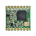
RF Transceiver Module RFM69W 868MHZ
The RFM69W is a transceiver module capable of operation over a wide frequency range, including the 868 Mhz license-free ISM (Industry Scientific and Medical) frequency bands. All major RF communication parameters are programmable and most of them can be dynamically set. The RFM69W offers the unique advantage of programmable narrow-band and wide-band communication modes The RFM69W is optimized for low power consumption while offering high RF output power and channelized operation. Compliance ETSI and FCC regulations. In order to better use RFM69W modules, this specification also involves a large number of the parameters and functions of its core chip RF69's, including those IC pins which are not led out. All of these can help customers gain a better understanding of the performance of RFM69W modules, and enhance the application skills.
₹966.00
In stock
SKU
RF004-RFM69W-868S2

Feature and application:
Features:
-
+13 dBm Power Output Capability
-
High Sensitivity: down to -120 dBm at 1.2 kbps
-
High Selectivity: 16-tap FIR Channel Filter
-
Bullet-proof front end: IIP3 = -18 dBm, IIP2 = +35 dBm,80 dB Blocking Immunity, no Image
-
Frequency response
-
Low current: Rx = 16 mA, 100nA register retention
-
Programmable Pout: -18 to +13 dBm in 1dB steps
-
Constant RF performance over the voltage range of chip
-
FSK Bit rates up to 300 kb/s
-
Fully integrated synthesizer with a resolution of 61 Hz
-
FSK, GFSK, MSK, GMSK and OOK modulations
-
Built-in Bit Synchronizer performing Clock Recovery
-
Incoming Sync Word Recognition
-
115 dB+ Dynamic Range RSSI
-
Automatic RF Sense with ultra-fast AFC
-
Packet engine with CRC-16, AES-128, 66-byte FIFO
-
Built-in temperature sensor
Applications:
-
Automated Meter reading
-
Wireless Sensor Networks
-
Home and Building Automation
-
Wireless Alarm and Security Systems
-
Industrial Monitoring and Control
-
Wireless M-BUS
Block diagram:

Pin and marking diagram:
The following diagram shows the pin arrangement, top view.

Pin description:
|
Number |
Name |
Type |
Description |
|
1 |
RESET |
I/O |
Reset trigger input |
|
2 |
DIO0 |
I/O |
Digital I/O, software configured |
|
3 |
DIO1 |
I/O |
Digital I/O, software configured |
|
4 |
DIO2 |
I/O |
Digital I/O, software configured |
|
5 |
DIO3 |
I/O |
Digital I/O, software configured |
|
6 |
DIO4 |
I/O |
Digital I/O, software configured |
|
7 |
DIO5 |
I/O |
Digital I/O, software configured |
|
8 |
3.3V |
- |
Supply voltage |
|
9 |
GND |
- |
Ground |
|
10 |
ANA |
RF Signal input/output |
|
|
11 |
GND |
- |
Ground |
|
12 |
SCK |
I |
SPI Clock input |
|
13 |
MISO |
O |
SPI Data output |
|
14 |
MOSI |
I |
SPI Data input |
|
15 |
NSS |
I |
SPI Chip select input |
|
16 |
NC |
- |
Connect to GND |
Electrical characteristics:
Absolute maximum ratings:
Stresses above the values listed below may cause permanent device failure. Exposure to absolute maximum ratings for extended periods may affect device reliability.
|
Symbol |
Description |
Min |
Max |
Unit |
|
VDDmr |
Supply Voltage |
-0.5 |
3.9 |
V |
|
Tmr |
Temperature |
-55 |
+115 |
° C |
|
Tj |
Junction temperature |
- |
+125 |
° C |
|
Pmr |
RF Input Level |
- |
+6 |
dBm |
|
DC_13dBm |
Duty Cycle of transmission at +13dBm output |
- |
1 |
% |
|
VSWR_13dBm |
Maximum VSWR at the antenna port |
- |
3:1 |
- |
Operating Range:
|
Symbol |
Description |
Min |
Max |
Unit |
|
VDDop |
Supply voltage |
1.8 |
3.6 |
V |
|
Top |
Operational temperature range |
-40 |
+85 |
°C |
|
Clop |
Load capacitance on digital ports |
- |
25 |
pF |
|
ML |
RF Input Level |
- |
0 |
dBm |
Power consumption:
|
Symbol |
Description |
Conditions |
Min |
Typ |
Max |
Unit |
|
IDDSL |
Supply current in Sleep mode |
- |
0.1 |
1 |
uA |
|
|
IDDIDLE |
Supply current in Idle mode |
RC oscillator enabled |
- |
1.2 |
- |
uA |
|
IDDST |
Supply current in Standby mode |
Crystal oscillator enabled |
- |
1.25 |
1.5 |
mA |
|
IDDFS |
Supply current in Synthesizer mode |
- |
9 |
- |
mA |
|
|
IDDR |
Supply current in Receive mode |
- |
16 |
- |
mA |
|
|
IDDT |
Supply current in Transmit mode with appropriate matching, stable across VDD range |
on RFIO pin, RFOP=+13 dBm RFOP = +10 dBm RFOP = 0 dBm, RFOP = -1 dBm |
- - - - |
45 33 20 16 |
- - - - |
mA mA mA mA |
Receiver:
|
Symbol |
Description |
Conditions |
Min |
Typ |
Max |
Unit |
|
RFS_F |
FSK sensitivity, the highest LNA gain |
FDA = 5 kHz, BR = 1.2 kb/s FDA = 5 kHz, BR = 4.8 kb/s FDA = 40 kHz, BR = 38.4 kb/s |
- - - |
-118 -114 -105 |
- - - |
dBm dBm dBm |
|
FDA = 5 kHz, BR = 1.2 kb/s * |
- |
-120 |
- |
dBm |
||
|
RFS_O |
OOK sensitivity, the highest LNA gain |
BR = 4.8 kb/s |
- |
-112 |
-109 |
dBm |
|
CCR |
Co-Channel Rejection |
-13 |
-10 |
- |
dB |
|
|
ACR |
Adjacent Channel Rejection |
Offset = +/- 25 kHz Offset = +/- 50 kHz |
-37 |
42 42 |
- - |
dB dB |
|
BI |
Blocking Immunity |
Offset = +/- 1MHz Offset = +/- 2 MHz Offset = +/- 10MHz |
- - - |
66 71 79 |
- - - |
dB dB dB |
|
AMR |
AM Rejection, AM modulated interferer with 100% modulation depth, FM = 1 kHz, square |
Offset = +/- 1MHz Offset = +/- 2 MHz Offset = +/- 10MHz |
66 71 79 |
- - - |
dB dB dB |
|
|
IIP2 |
2nd order Input Intercept Point Unwanted tones are 20 MHz above the LO |
Lowest LNA gain Highest LNA gain |
- - |
+75 +35 |
- - |
dBm dBm |
|
IIP3 |
3rd order Input Intercept point Unwanted tones are 1MHz and 1.995 MHz above the LO |
Lowest LNA gain Highest LNA gain |
- -23 |
+13 -18 |
- - |
dBm dBm |
|
BW_SSB |
Single Side-channel filter BW |
Programmable |
2.6 |
- |
500 |
kHz |
|
IMR_OOK |
Image rejection in OOK mode |
Wanted signal level = -106 dBm |
27 |
30 |
- |
dB |
|
TS_RE |
Receiver wake-up time, from PLL, locked state toRxReady |
RxBw= 10 kHz,BR = 4.8 kb/s RxBw= 200 kHz, BR = 100 kb/s |
- - |
1.7 96 |
- - |
ms us |
|
TS_RE_AGC |
Receiver wake-up time, from PLL, locked state, AGC enabled |
RxBw= 10 kHz, BR = 4.8 kb/s RxBw= 200 kHz, BR = 100 kb/s |
- |
3.0 163 |
ms us |
|
|
TS_RE_AGC &AFC |
Receiver wake-up time, from PLL lock state, AGC and AFC enabled |
RxBw= 10 kHz, BR = 4.8 kb/s RxBw= 200 kHz, BR = 100 kb/s |
4.8 265 |
ms us |
||
|
TS_FEI |
FEI sampling time |
Receiver is ready |
- |
4.Tbit |
- |
- |
|
TS_AFC |
AFC Response Time |
Receiver is ready |
- |
4.Tbit |
- |
- |
|
TS_RSSI |
RSSI Response Time |
Receiver is ready |
- |
2.Tbit |
- |
- |
|
DR_RSSI |
RSSI Dynamic Range |
- - |
-115 0 |
- - |
dBm dBm |
Transmitter:
|
Symbol |
Description |
Conditions |
Min |
Typ |
Max |
Unit |
|
RF_OP |
RF output power in 50 ohms On RFIO pin |
Programmable with1dBsteps |
- - |
+13 -18 |
- - |
dBm dBm |
|
- |
||||||
|
ΔRF_OP |
RF output power stability |
From VDD=2.4V to 3.6V |
- |
+/-0.3 |
- |
dB |
|
PHN |
Transmitter Phase Noise |
50 kHz Offset from the carrier 868 / 915 MHz bands 434 / 315 MHz bands |
- - |
-95 -99 |
- - |
dBc/ Hz |
|
ACP |
Transmitter adjacent channel power (measured at 25 kHz offset) |
BT=0.5 . Measurement conditions as defined by EN 300 220-1 V2.1.1 |
- |
- |
-37 |
dBm |
|
TS_TR |
Transmitter wake up time, to the first rising edge of DCLK |
Frequency Synthesizerenabled, PaRamp= 10 us, BR = 4.8kb/s. |
- |
120 |
- |
us |
| Subtitle | N/A |
|---|---|
| UPC/EAN | 4604046160306 |
| Count | 1 |
| M.R.P | ₹1,440.00 |
| Brand Name | HopeRF |
| Model | RFM69W-868MHZ |
| Whoesale | Available |
| Frequency | 868 MHz |
| Color | Green |
| Modulations | FSK, GFSK, MSK, GMSK and OOK |
| FSK Bit rates | 300 kb/s |
| Demodulations | N/A |
| Dimension | 19.7X16mm |
Write Your Own Review
Featured